Queen Mary University of London
QMUL has extensive facilities for materials processing, materials characterisation and device fabrication. This includes a clean room, photolithography, Raman spectroscopy, ellipsometry, X-ray and ultraviolet photoelectron spectroscopy (XPS and UPS), ion scattering spectroscopy (ISS), reflected electron energy loss spectroscopy (REELS) and a suite of optical microscopes, atomic force microscopes (AFM) and transmission/scanning electron microscopes (TEM/SEM). QMUL is applying for the latest 2D MOCVD growth system. QMUL also houses a Nanoscribe 3D laser lithography system that provides a fast and powerful platform for sub-µm resolution micro and nanofabrication, with a writing area of up to 100 × 100 mm2 and 3 mm height.
Summary of Key Facilities at Queen Mary University of London:
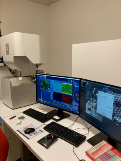
JEM-F200 Scanning Transmission Electron Microscope
JEM-1400 Flash Transmission Electron Microscope (Details on TEMs)
ThermoFisher Nexsa for X-ray Photoelectron Specoscopy (XPS), Reflected Electron Energy Loss Spectroscopy (REELS), Ultraviolet Photoelectron Spectroscopy (UPS) and Ion Scattering Spectroscopy (ISS).
Renishaw inVia Reflex Spectrometer System for Raman StreamLineTM spectral analysis and rapid imaging system. (Available laser wavelengths: 442 nm, 532 nm, 633 nm and 785 nm)
Linseis Thin Film Analyser for measurement of themal conductivity, electrical conductivity and Seebeck coefficient (100K-450K)
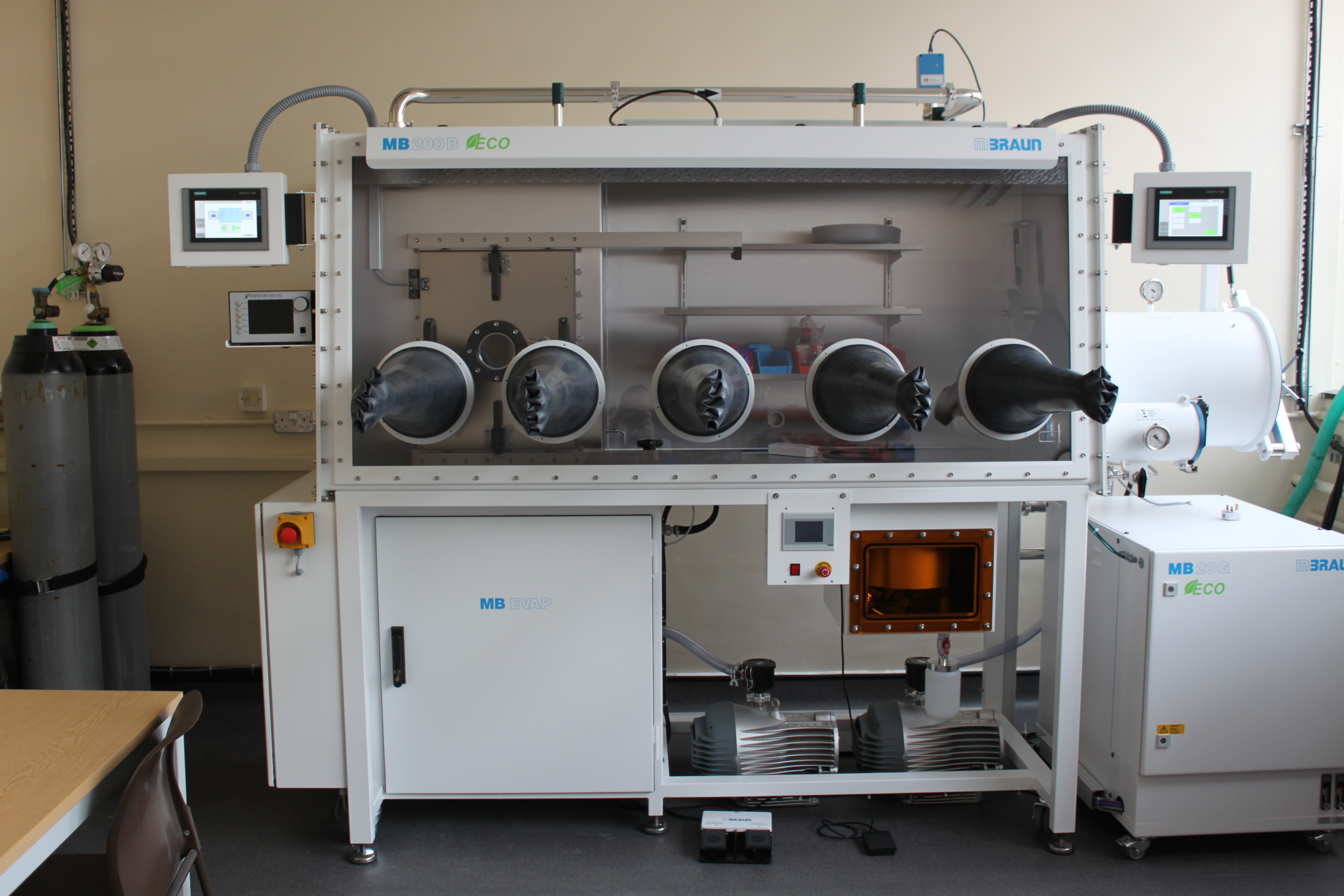
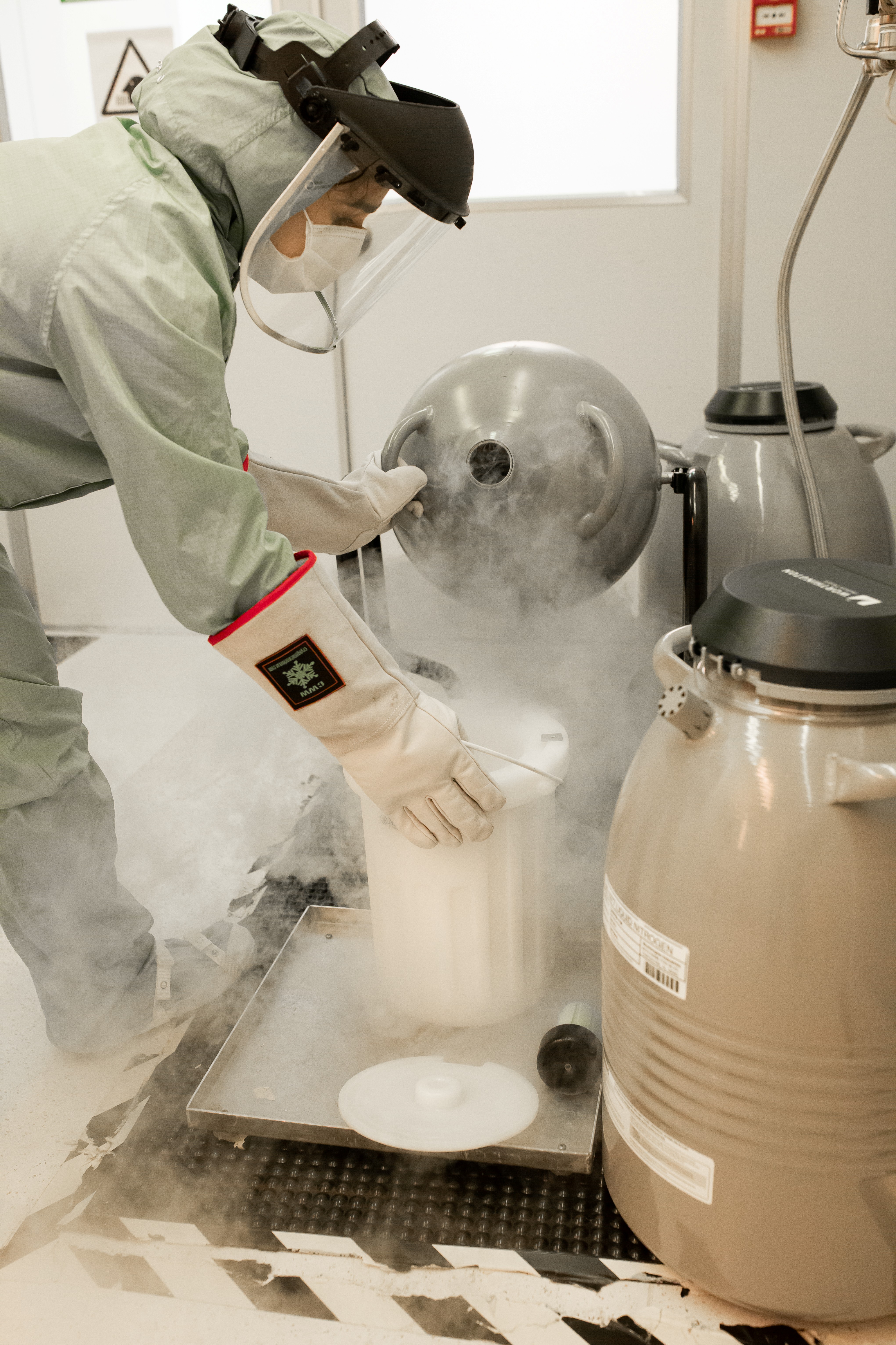
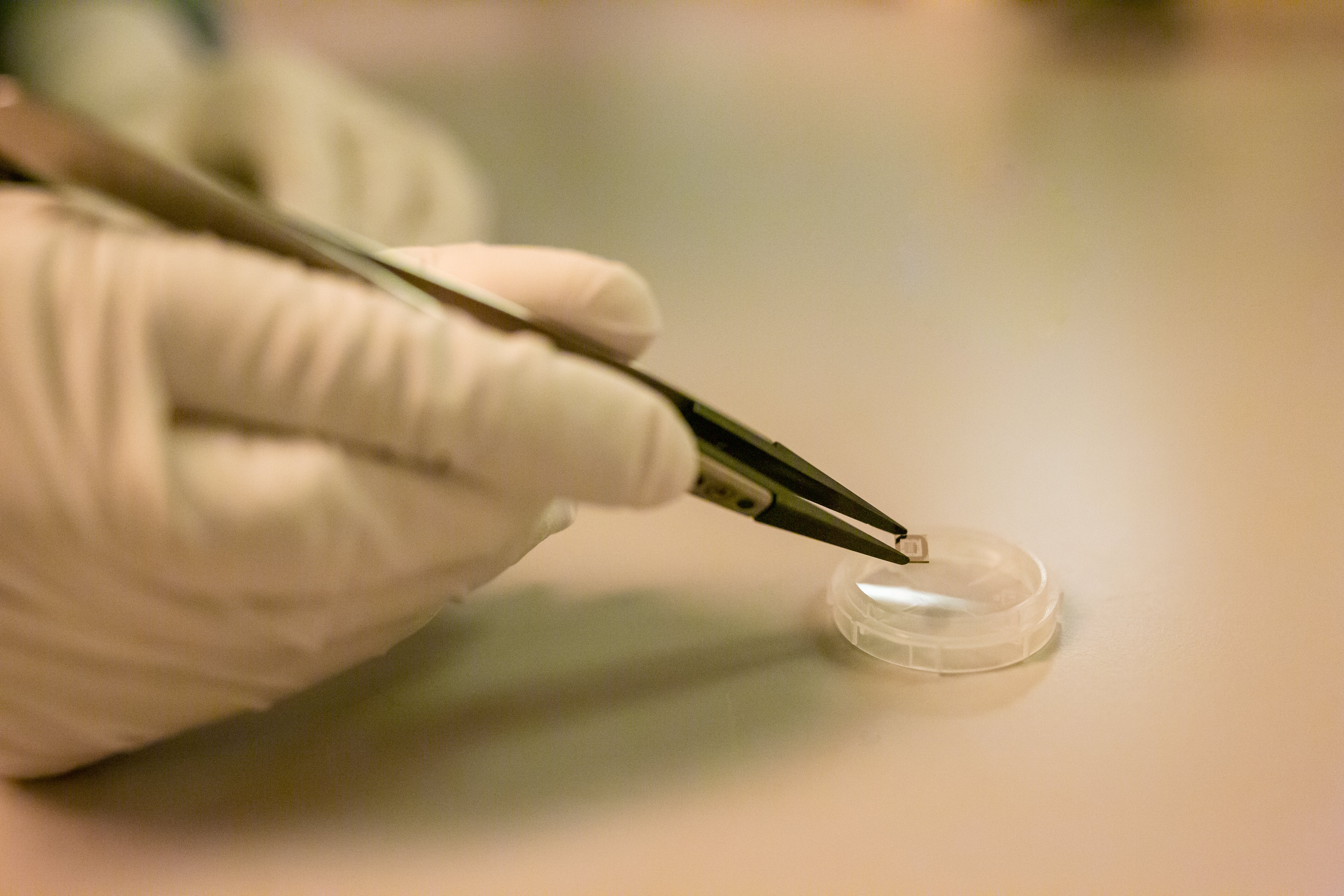
Gloveboxes for sensitive sample handling.
Bruker Icon Atomic Force Microscope (AFM) fitted with Kelvin Probe Force Microscopy (KPFM), conductive AFM (C-AFM), piezo force microscopy (PFM), nanomechanical analysis and more.
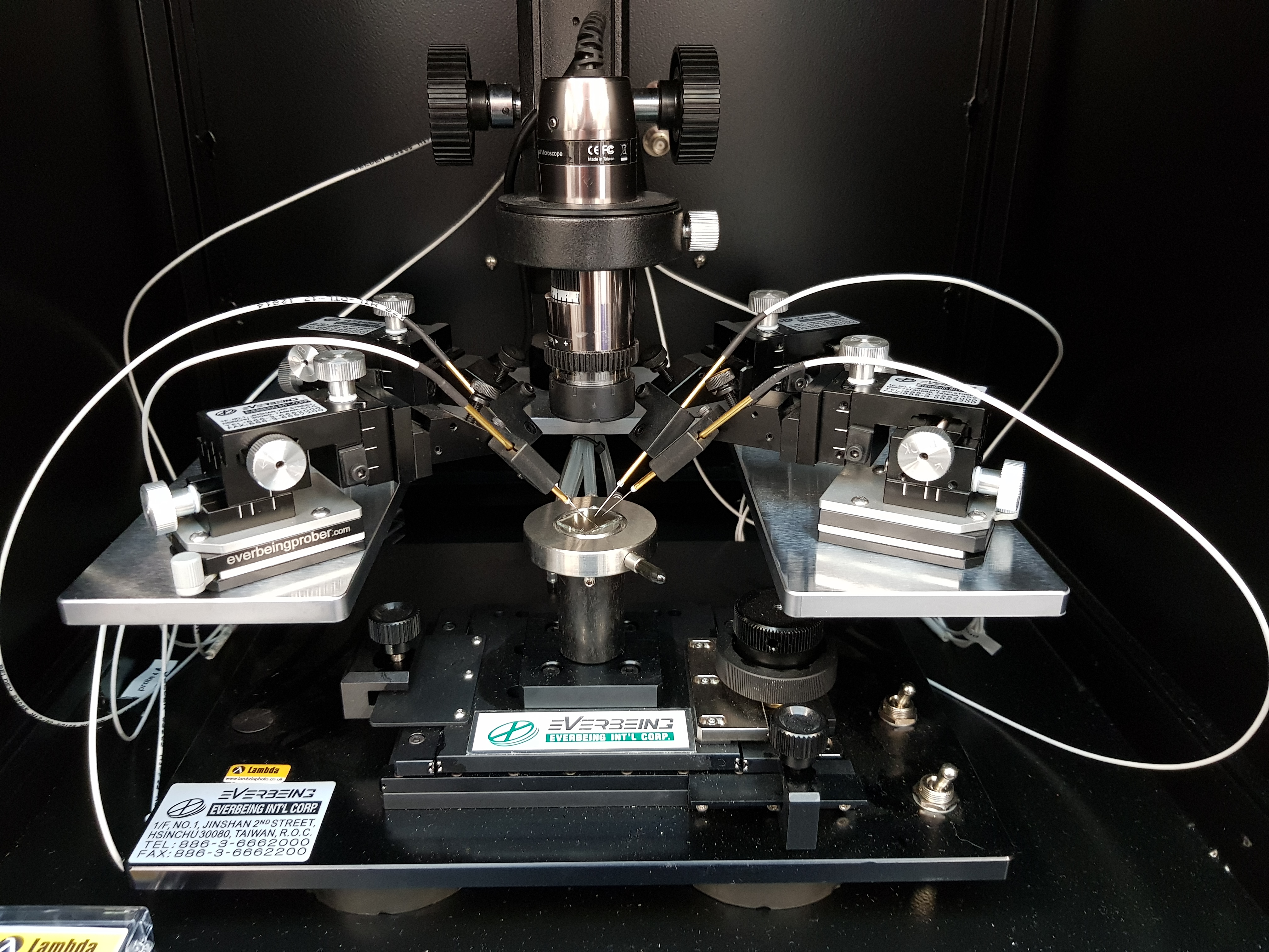
Probe station for electrical characterization.
University of Glasgow
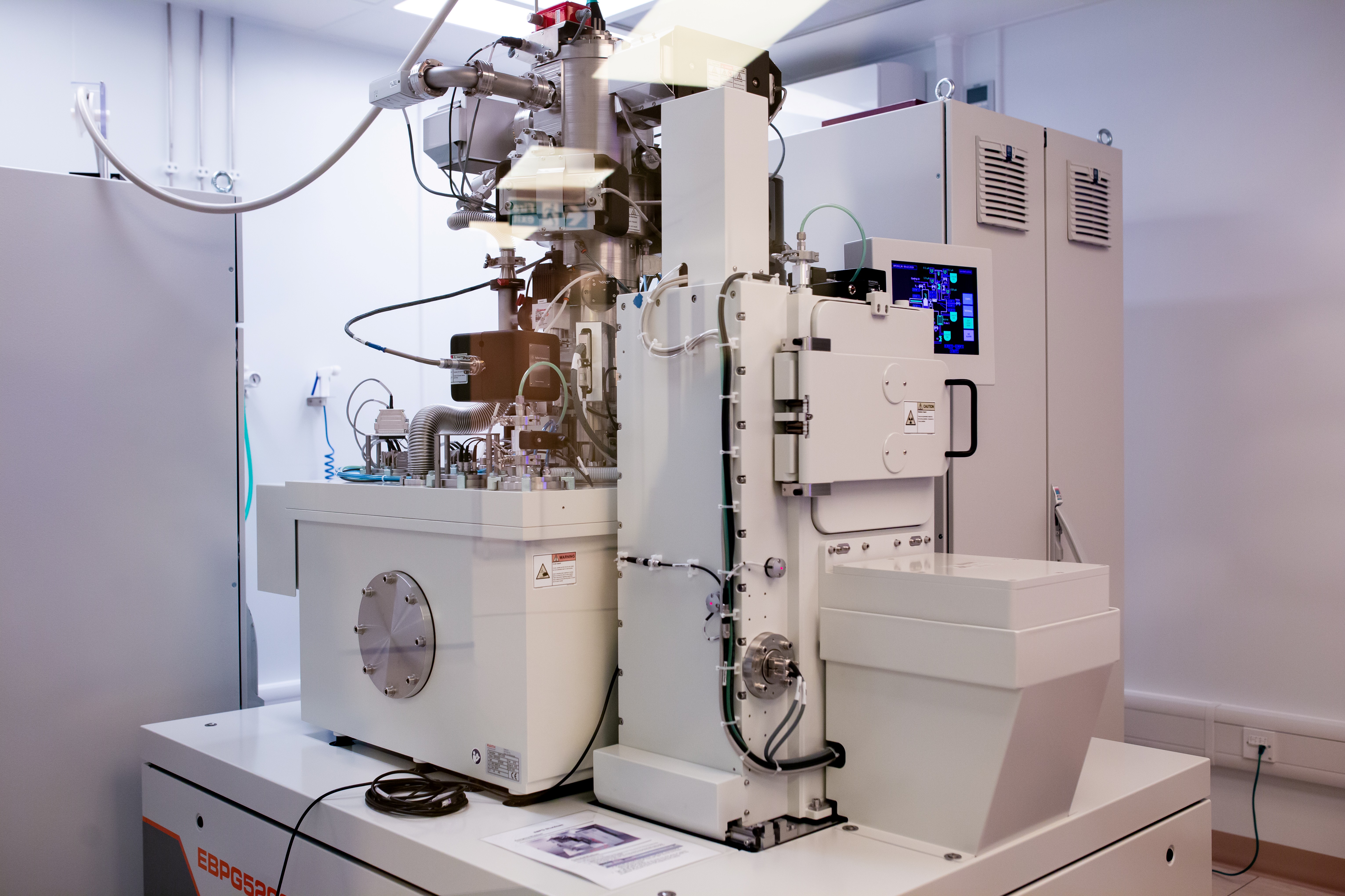
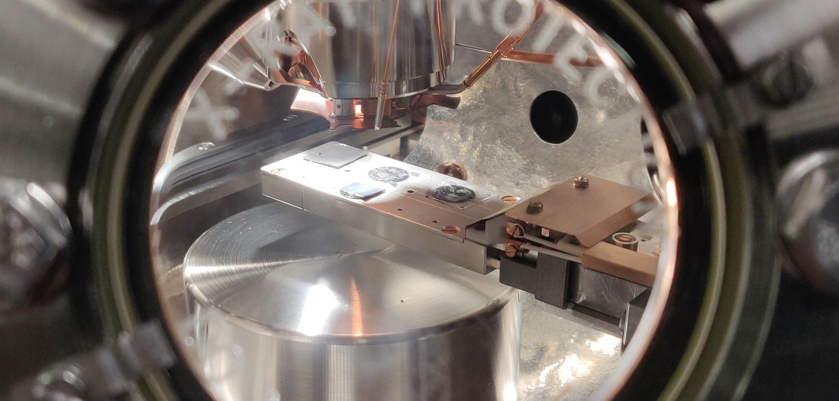
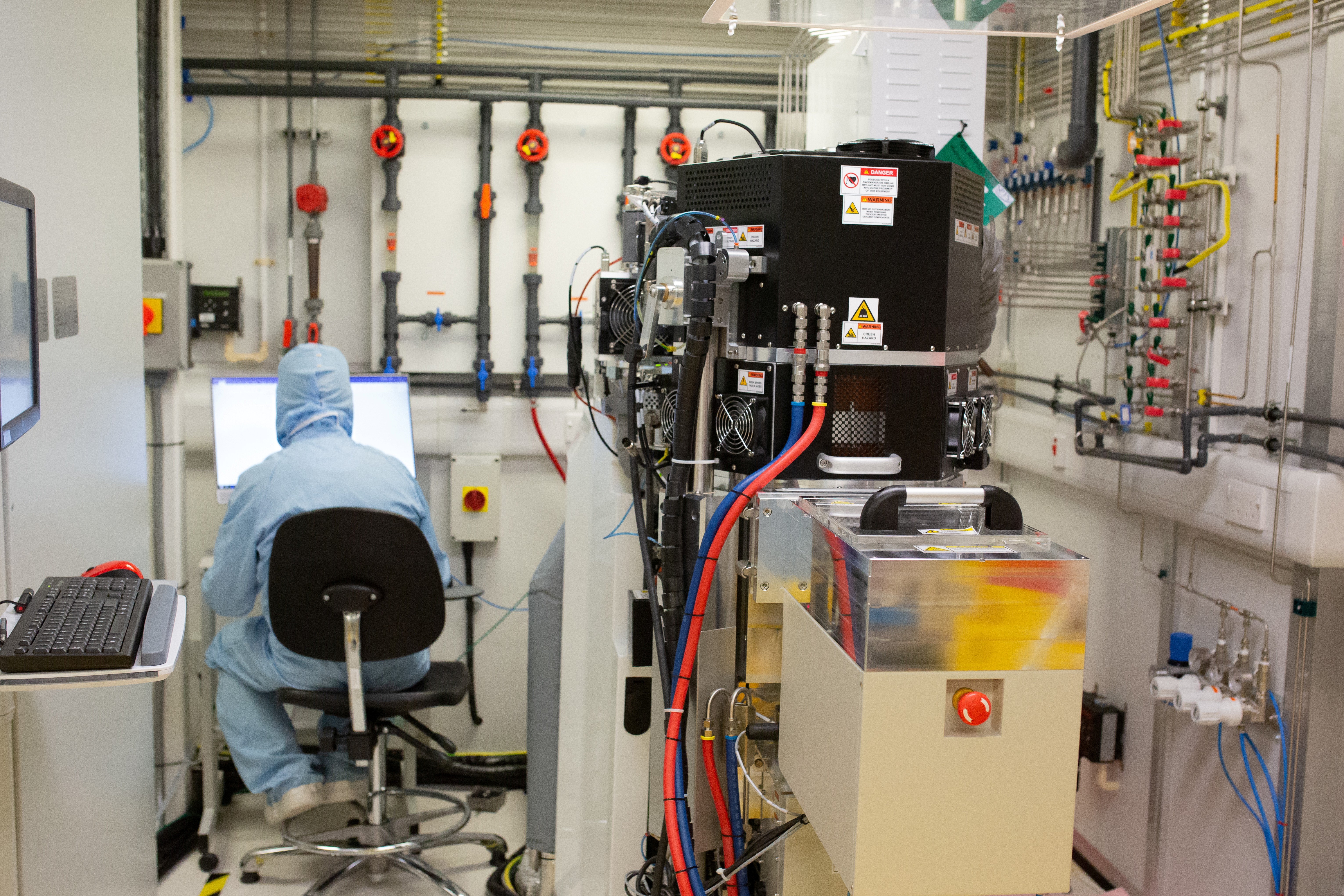
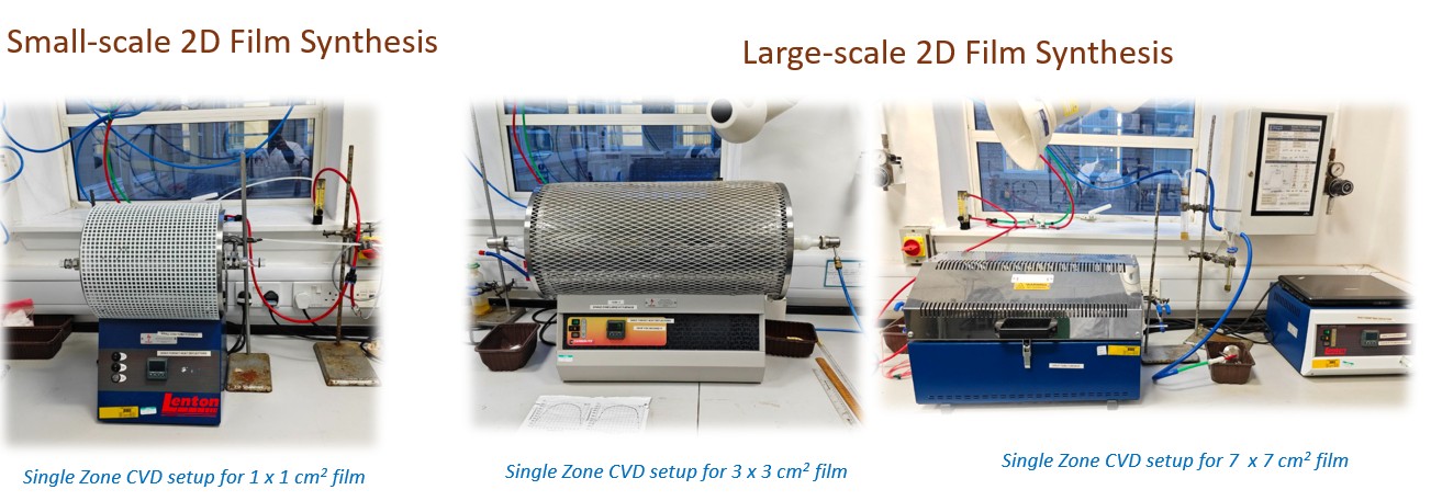
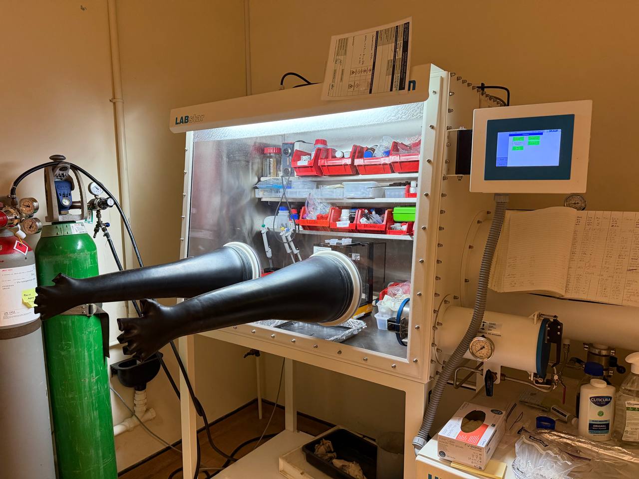
The James Watt Nanofabrication Centre (JWNC) at the University of Glasgow (UoG) is a £32M 1400 m2 cleanroom facility supported by 28 technical staff and home to the various lithography, processing and analysis tools required to undertake the fabrication components of the project. This includes electron-beam and photolithography providing feature size definition down to 10 nm, various metal and dielectric deposition tools (electron-beam, thermal and Atomic Layer Deposition), more than 15 systems plasma tools which provide access to a range of surface processing and dry-etch chemistries, and various characterisation capability including electron microscopy, EDX, optical microscopy, scanning probe microscopy, Auger, Raman, XPS and electrical Hall measurement. The deposition facilities in JWNC are seamlessly integrated with several CVD setups in the School of Chemistry at UoG which has access to a large variety of special gases (H2, CH4 and NH3) and small molecules to enable 2DSEM surface functionalisation. The CVD access leverages the proximity to the SEM Tescan microscopy suit recently installed as well as the unique electron diffraction facility. Access to several gloveboxes within the School warrants that any issues with air exposure are contained. This UoG capability has been used for CVD growth and device processing based on various 2DSEM techniques.
University of Nottingham
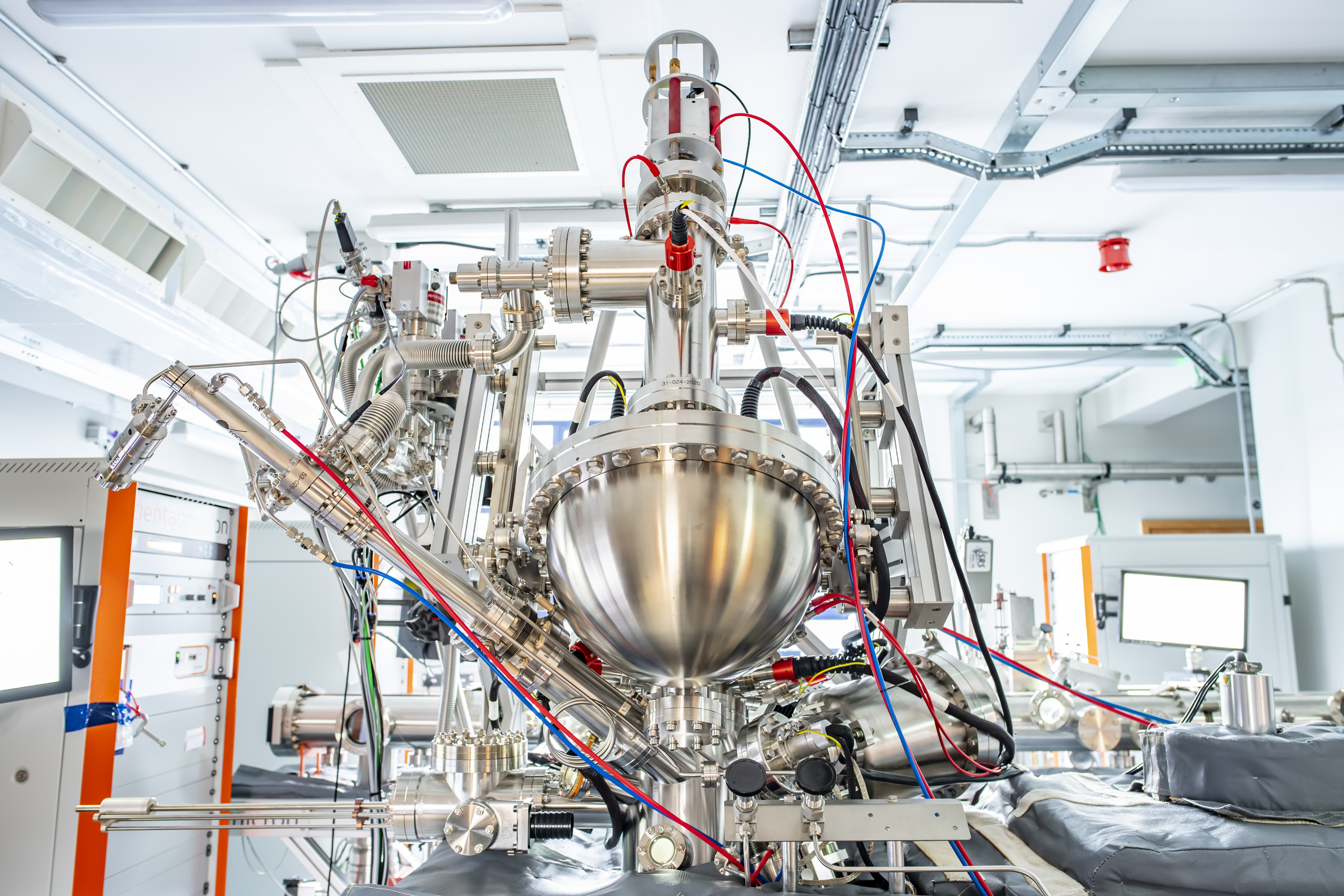
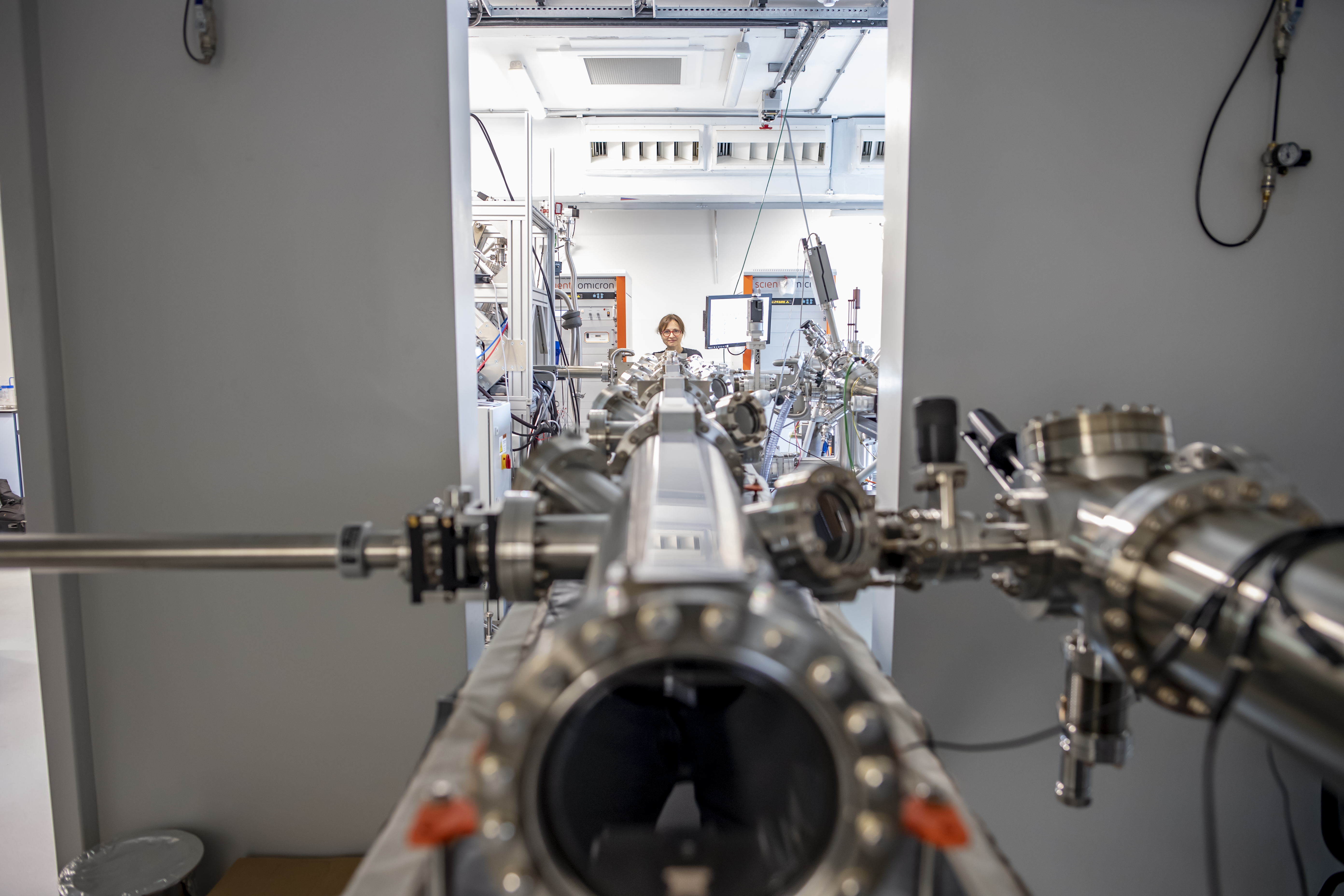
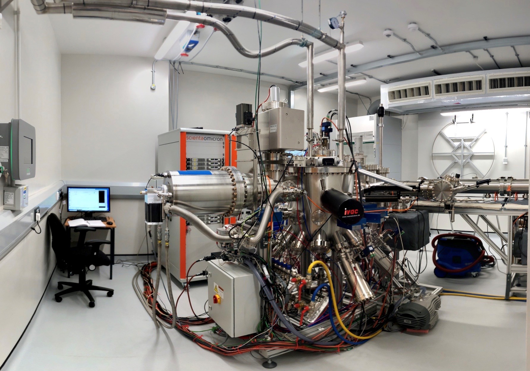
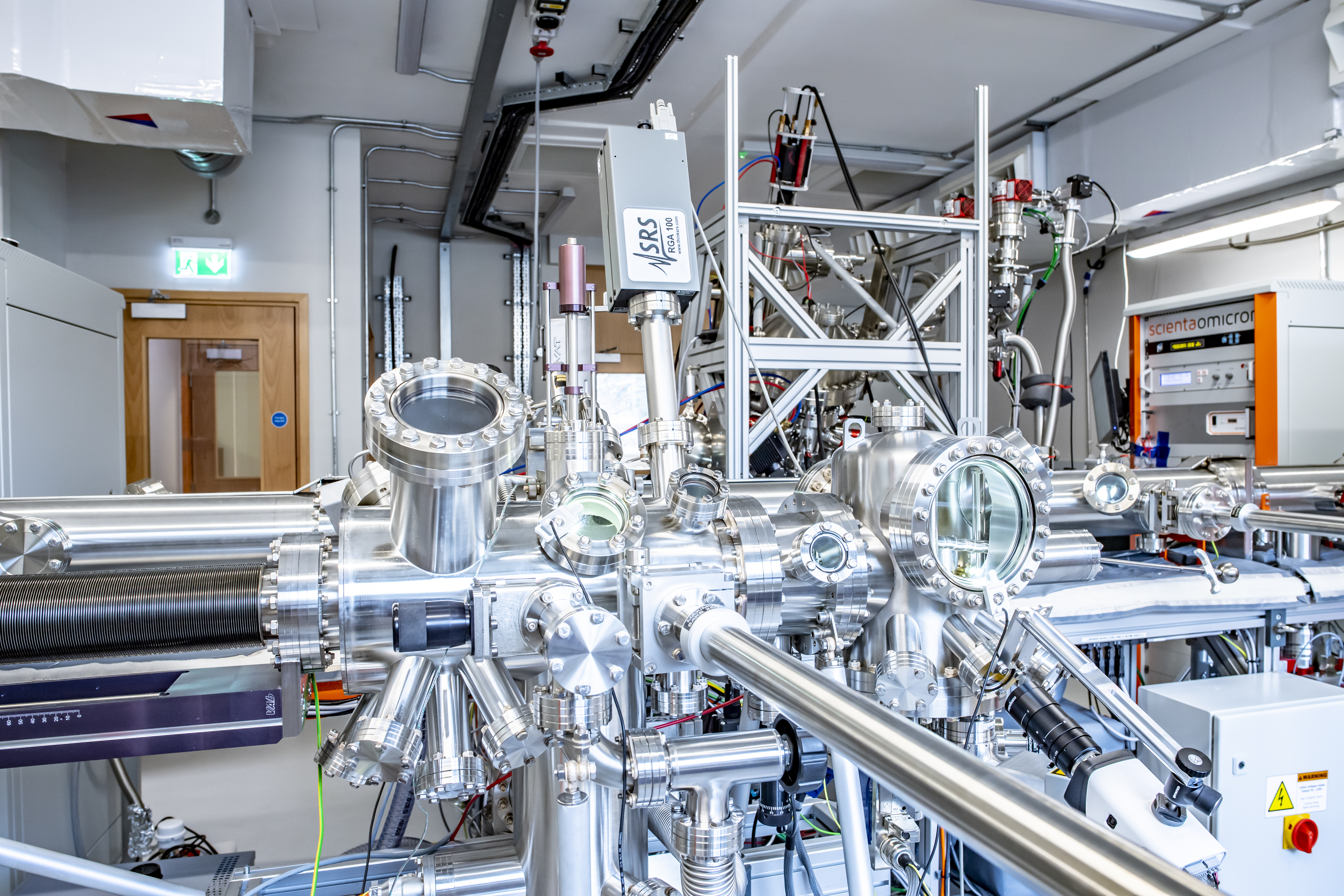
At the University of Nottingham, we use state-of-the-art manufacturing technologies to advance the precise engineering of 2DSEM. Our facility, EPI2SEM, comprises a custom-designed MBE reactor and in situ UHV (ultra-high vacuum) analytical techniques.
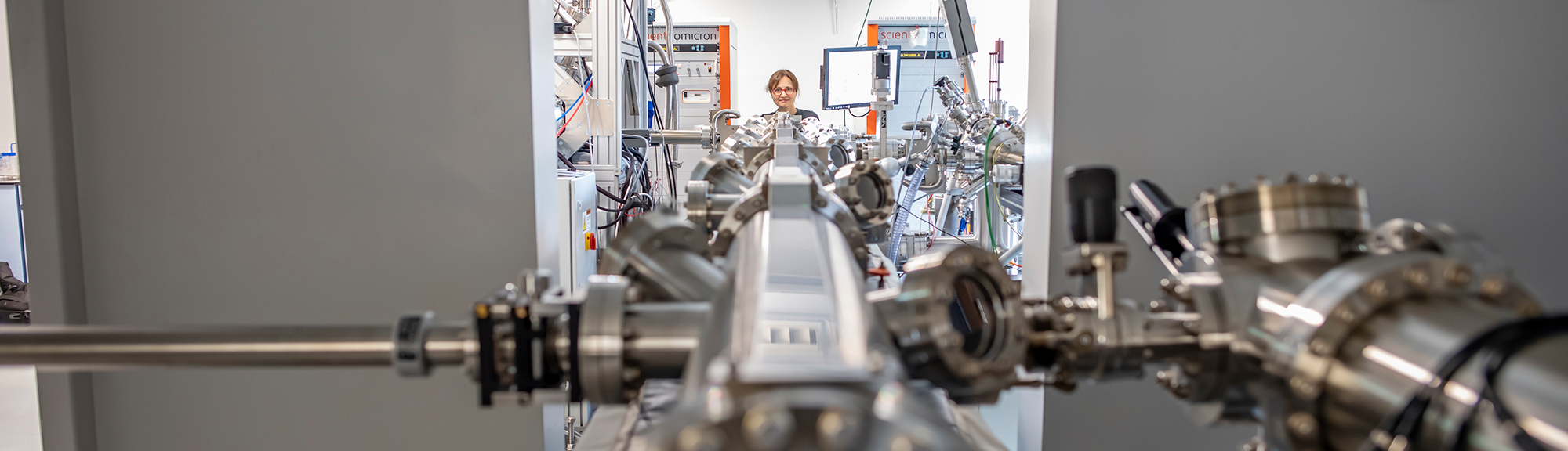
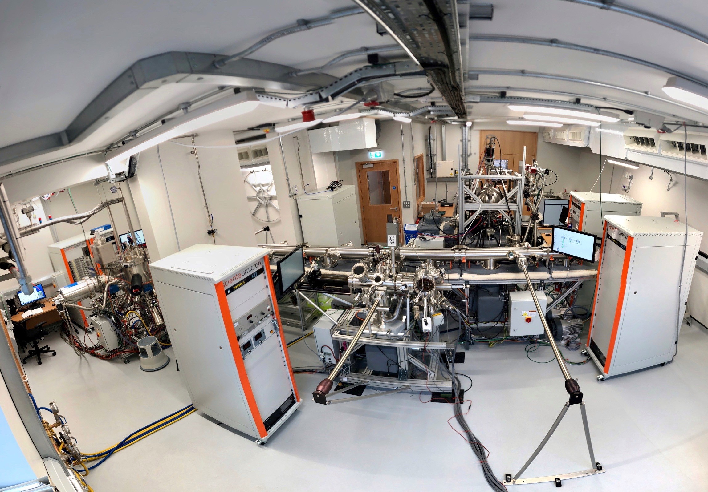
These include scanning probe microscopy (SPM) and electron spectroscopy for chemical analysis (ESCA). The ESCA is a multi-platform instrument for chemical analysis by: XPS (X-ray Photoelectron Spectroscopy) with high spatial resolution (<0.5 µm); PEEM (Photoemission Electron Microscopy) in real-time with nanometer resolution (< 40 nm); micro-Angle-Resolved Photoemission Spectroscopy (µ-ARPES) with high energy (<0.02 eV) and spatial (µm) resolution for band structure and Fermi surface mapping in k-space. Surface geometry, morphology and reconstructions are determined by Scanning Tunnelling Microscopy, STM, and Atomic Force Microscopy, AFM.