Materials -> Processes -> Devices -> Impact
Approach map
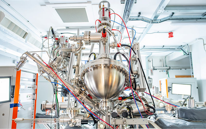
Atomic scale designs
Exploring device concepts and architectures that exploit atomically thin materials and their interfaces, with attention to scalability and manufacturable routes.
Why our approach is effective
NEED2D links materials creation, theory, and device fabrication in a single programme so discoveries translate rapidly into measurable device-level gains. The approach is designed to resolve interdependent barriers (growth quality, interfaces, contacts, electrostatics) that cannot be solved in isolation.
Why our project is feasible
The programme builds on established UK capability in wafer-scale 2D materials, advanced characterisation, and device prototyping. The consortium’s complementary expertise provides multiple routes to validate and scale results.
Risks and mitigations
NEED2D links materials creation, theory, and device fabrication in a single programme so discoveries translate rapidly into measurable device-level gains. The approach is designed to resolve interdependent barriers (growth quality, interfaces, contacts, electrostatics) that cannot be solved in isolation.
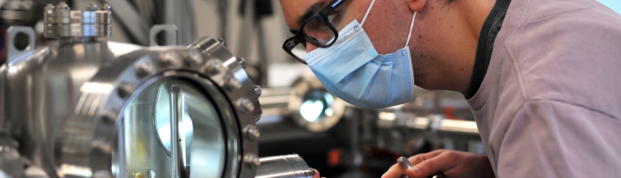
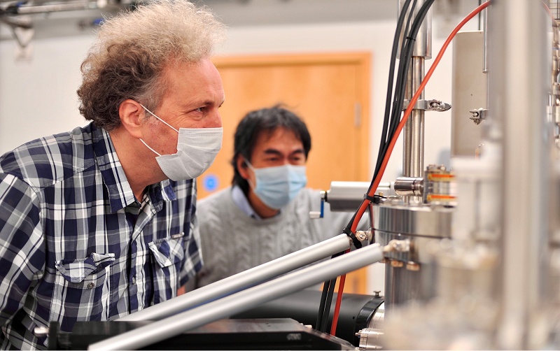
Research environments
The consortium’s research environments provide complementary facilities, technical leadership, and training capability. Shared methods and comparisons support reproducibility across sites.
Additionality
A coherent long-term programme enables flexibility, scale and sustained collaboration—supporting breakthroughs that would be unlikely through shorter, fragmented grants.
Added value and coherence
NEED2D’s structure supports coherence across disciplines and sustained, iterative progress. The longer-term nature of the programme allows the community to converge on reproducible, scalable routes while training the next generation of experts.