A Clear Pathway
From energy pressure to engineered devices
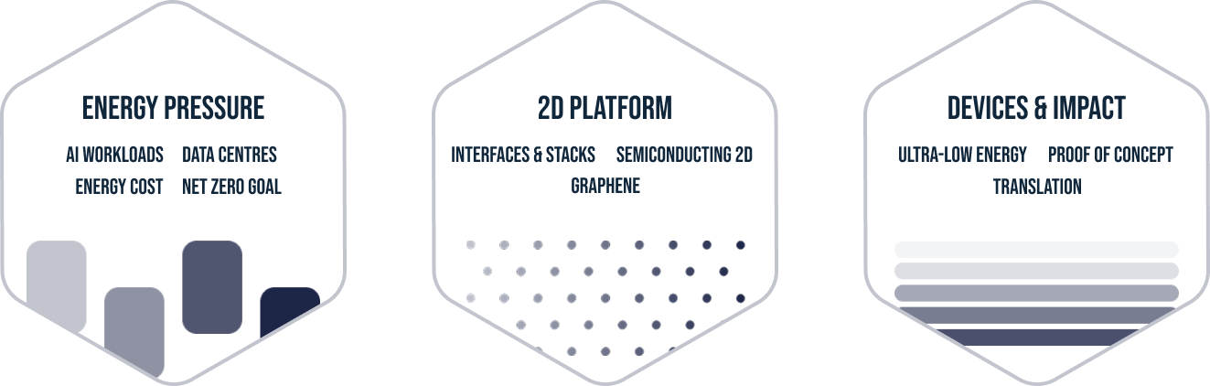
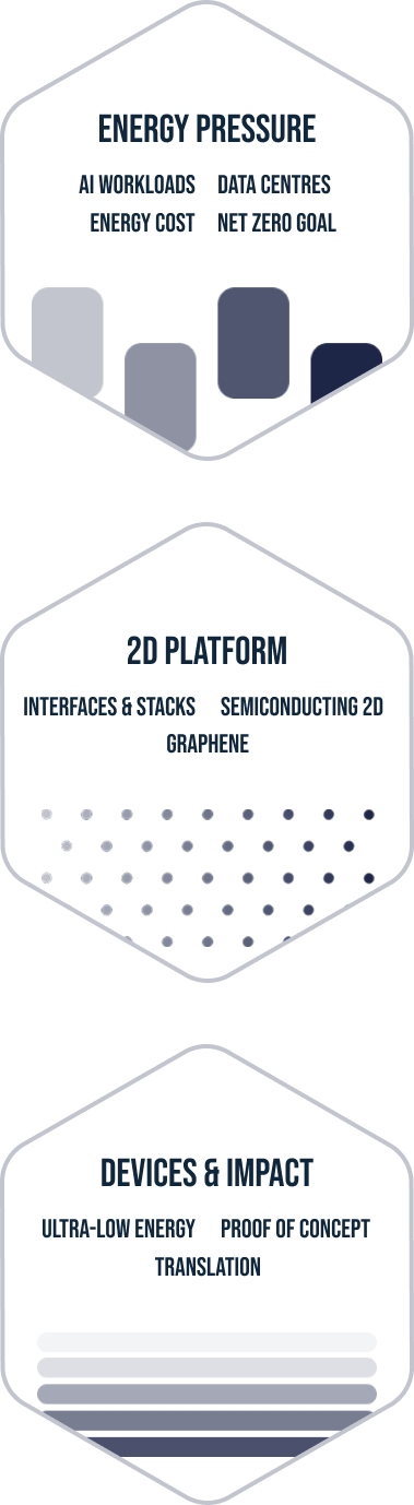
Timeliness: AI, data centres & energy
The expansion of AI workloads and data infrastructure is increasing electricity demand and elevating energy efficiency to a first-order constraint for future computing.
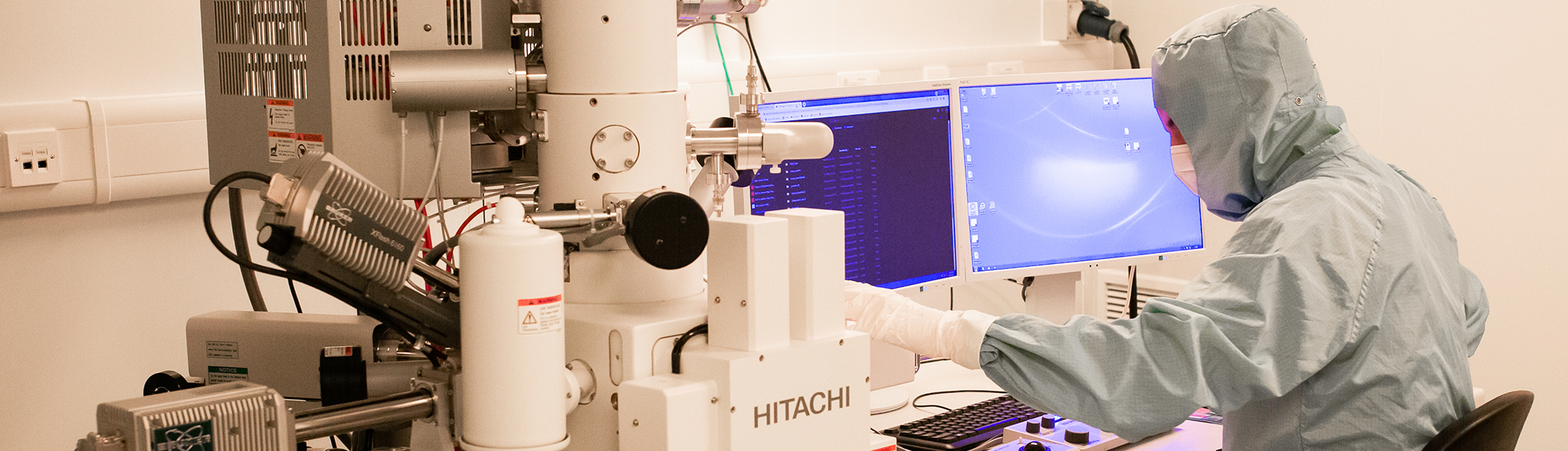
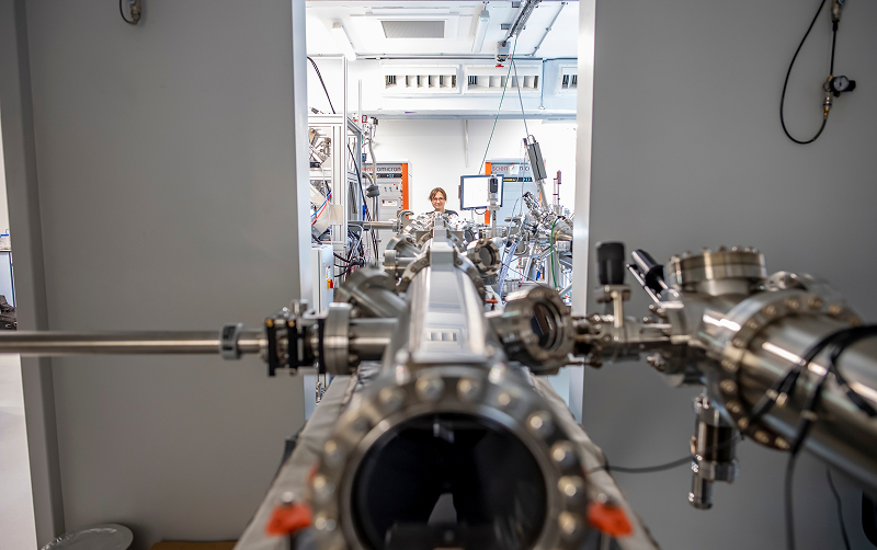
Interfaces dominate at atomic thickness: trapped charges, scattering and contact resistance can outweigh intrinsic advantages.
Overall vision
A new class of manufacturable devices built from atomically thin materials. By combining 2D layers into engineered heterostructures, NEED2D targets functionality and performance beyond conventional semiconductors.
Layer-by-layer design enables control of electrostatics, band alignment and interfaces, improving leakage control and contact behaviour.
Advancing understanding
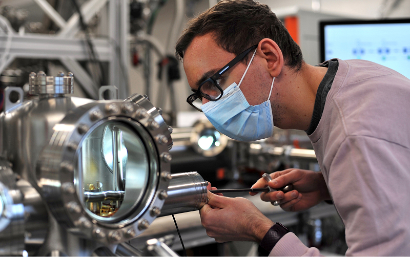
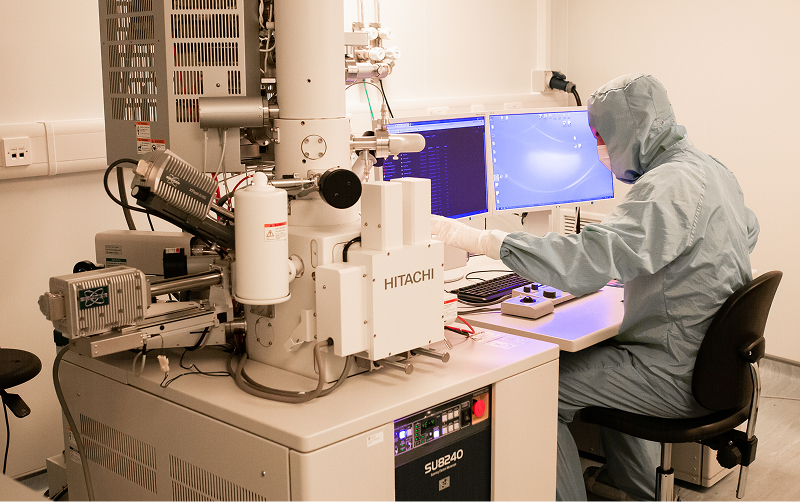
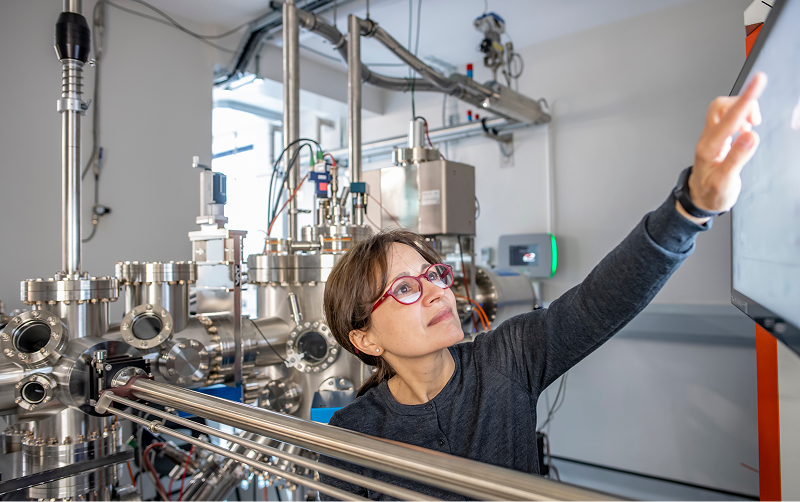
Identify limits from defects, interfaces and contacts and establish how to stack 2D layers without degrading performance—essential for reliable, reproducible devices.
Interfaces dominate at atomic thickness: trapped charges, scattering and contact resistance can outweigh intrinsic advantages.
Impact
Ultra-low-energy electronics can reduce emissions from digital infrastructure, enable sustainable AI growth, and catalyse high-value UK innovation and capability.
Impact combines environmental leverage (energy reduction) with economic leverage (sovereign post-silicon capability).